PRGA Workflow
A typical PRGA workflow consists of three major steps:
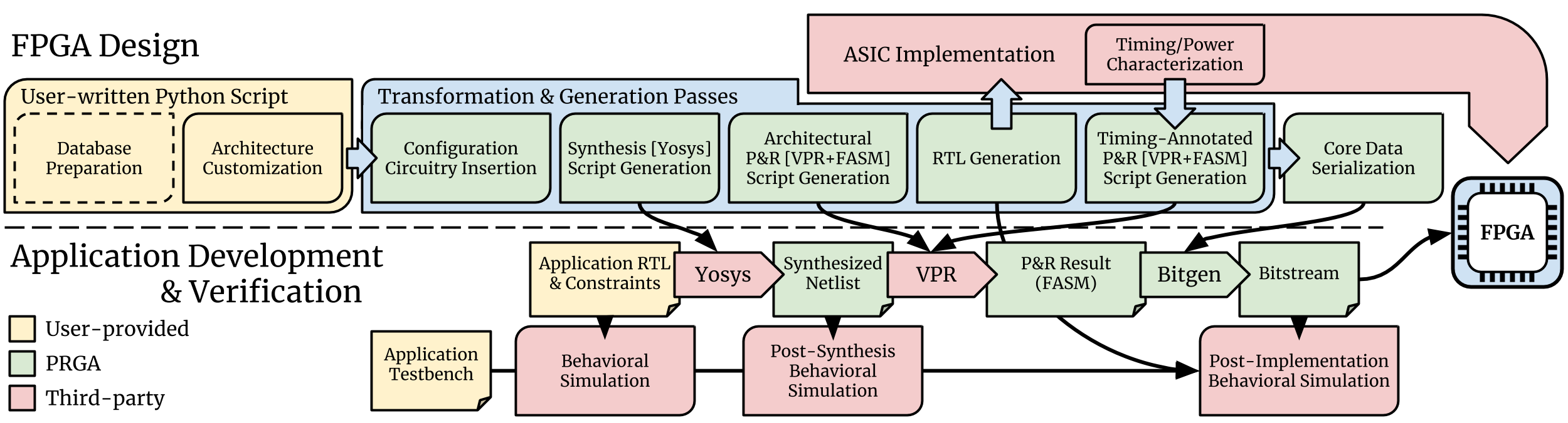
- FPGA Design: Design and customize FPGA architecture, then generate ASIC-compatible RTL for the FPGA. PRGA also generates all the CAD scripts needed by the Application Development step.
- Application Development: Use Yosys and VPR to synthesize, place and route an RTL application, then use PRGA to generate the bitstream for the custom FPGA.
- Incremental Verification: Run behavioral simulation with user-provided testbench, then post-synthesis (LUT-based) simulation, and ultimately full-fabric, post-implementation simulation.
FPGA Design
The first major step, FPGA Design flow, is driven by a user-written Python script using the PRGA API. Example scripts can be found and ran under the examples/fpga directory. More information can be found at Tutorials.
In the Python script, the FPGA designer first describes and customizes the
desired FPGA architecture at an abstract, functional level, without concerning
about the underlying configuration memory or the physical implementation.
After specifying the architecture, a Flow of various Pass es are applied
to automatically complete the rest of the FPGA Design flow.
The abstract connections and modules are automatically implemented with
RTL modules.
Configuration memories are also automatically inserted according to the number
of configuration bits needed per block.
Then, ASIC-compatible RTL files are generated for the custom FPGA, as well as
the Yosys and VPR scripts.
Architecture Context
All PRGA data in the Python script are managed in a Context object, which can
be serialized and stored on hard disks, then recovered at any time.
For example, in examples/fpga/pktchain/fpga21/build.py, the Context is
cached after generating the Yosys and VPR scripts but before RTL
generation.
This enables a fast RTL re-generation when only the RTL templates are updated,
skipping the time-consuming VPR script generation step.
Database Preparation
PRGA offers various basic components for building an FPGA, including look-up tables (LUT), registres, adders, behavioral multipliers, behavioral SRAM models, etc. However, FPGA designers often want to add custom components into the FPGA, for example, real SRAM macros, hard arithmetic units, or even large, complex IP cores like hard CPUs, memory controllers, PCIe interfaces, etc. All these components are classified as Logic Primitive s in PRGA, and PRGA users can easily add custom Logic Primitive s at the beginning of their Python script. An example FPGA with a hard PicoRV32 CPU and custom negative-edge-triggered flipflops can be found at examples/fpga/magic/hardpico.
Architecture Customization
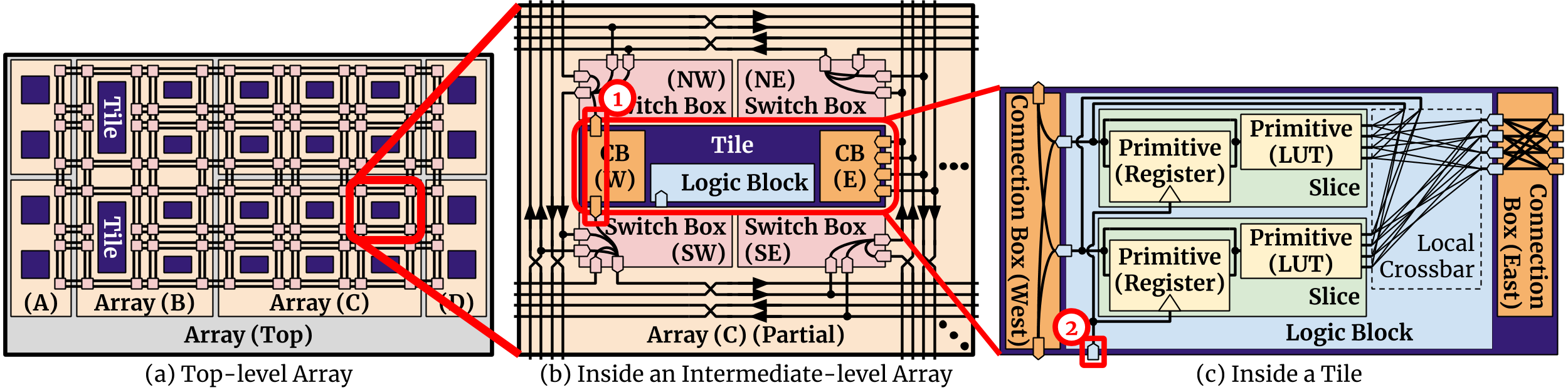
After database preparation, FPGA designers can design and customize the desired FPGA architecture by creating programmable blocks and assembling them in a hierarchical manner. As shown in the figure above, the FPGA is organized as a 2-dimensional Array of Tile s, Switch Box es, and nested Array s. Each Tile contains one Logic Block or multiple IO Block s, in addition to various numbers of Connection Box es. Each Logic Block or IO Block consists of zero to many Slice s and Logic Primitive s. Slice s are composed of nested Slice s and Logic Primitive s. Readers familiar with VPR should find these concept pretty intuitive. For more information, please refer to Architecture & Customizability.
One key feature of PRGA is the decoupling of the functional abstraction of an FPGA, the underlying configuration memory, and the physical implementation of the circuits. During architecture customization, FPGA designers can focus on describing the logical function and connectivity, and leave the implementation details to later steps, which are independently customizable. For example, to create a configurable connection in a logic block, FPGA designers only need to create a multi-source connection, without explicitly specifying how the MUX/BUFFER tree should be constructed.
This decoupling is enabled by using different ModuleView s of the same modules in
different steps.
This is covered in more detail in the Module View section.
During the architecture customization step, all modules are customized in
the abstract view.
Flow and Passes
PRGA does all the heavy-lifting job with transformation and generation
Pass es, which are Python objects with a run method to inspect or modify
the Context object.
Pass es are managed by a Flow object, which resolves the dependency,
conflict and ordering between Pass es.
Here’s a list of the most commonly used Pass es:
VPRArchGenerationandVPR_RRG_Generation: These two passes generate the VPR architecture specification and routing resource graph specification, respectively.YosysScriptsCollection: This pass inspects theContextobject and creates Yosys script generation tasks, including the main synthesis script, technology mapping script, block RAM inferrence script, and so on.Materialization: This pass adds the design view of the Logic Primitive s. Certain primitives may be implemented differently on different programming protocols, while some primitives are not supported by all programming protocols. For example, initializable memories that may be used as ROMs are only supported by theFrame-based programming protocol.Translation: This pass generates the design view for modules in the abstract view by linking Logic Primitive s and implementing the abstract configuratble connections with switch modules.SwitchPathAnnotation: This pass analyzes the switch modules instantiated in the design view, and annotate the MUX/BUFFER paths back to the abstract view. This information is used later by the bitstream generator.ProgCircuitryInsertion: This pass inserts configuration memory into the design view. This pass is specific to configuration circuitry types, e.g.Scanchain,PktchainandFrame, and only available after RTL generation tasks for all the modules in aFileRendererobject. RTL Verilog files are generated based on the design views.
File Rendering
VerilogCollection and YosysScriptsCollection passes do not generate the files
directly.
Instead, they create file rendering tasks in a FileRenderer object.
The FileRenderer object then generates all the files based on templates
written in Jinja.
To replace any PRGA-provided templates with custom templates (or plain text
files), simply add additional search paths to the FileRenderer object.
The first template found in the search paths will be used.
Generated Files
To use the automated CAD/verification flow to be covered in the
following sections, the Context object must be serialized onto hard disk:
ctx.pickle("ctx.pkl")
All the files required by the open-source FPGA CAD tools (Yosys and VPR) are generated in a complete FPGA design flow and can be reused when mapping different RTL applications onto the same FPGA. Below is an example structure of the generated files:
project/
 +- ctx.pkl                     # pickled (serialized) context
 +- rtl/
 |   +- top.v                   # human-readable Verilog RTL
 |   +- clb.v
 |   +- ...
 |   +- include/
 |       +- prga_utils.vh       # Verilog header files
 |       +- ...
 +- syn/
 |   +- read_lib.tcl            # Yosys pre-synthesis script
 |   +- synth.tcl               # Yosys synthesis script
 |   +- bram.rule               # Yosys BRAM inference rule
 |   +- m_adder.lib.v           # behavioral model for post-syn sim
 |   +- m_adder.techmap.v       # Yosys techmapping RTL
 |   +- ...
 +- vpr/
     +- arch.xml                # VPR arch spec
     +- rrg.xml                 # VPR RRG spec
ASIC Implementation
PRGA is designed and optimized with a strong emphasis on enabling gate-/transistor-level prototyping, or even fabrication, especially as a target of modern ASIC design flow with automated EDA tools and standard cell libraries. Although we cannot provide any production script, the generated RTL are intended to be ASIC-friendly. For example, the configuration enable and reset signals are registered at different levels across the hierarchy to reduce potential skew of these high-fanout nets; The LUTs and switches are deactivated during programming to minimize oscillation caused by combinational loops formed by partially programmed configuration memories. In addition, the flexible hierarchy and customizable RTL generation grant FPGA designers the freedom to explore and optimize ASIC implementation strategy specific to their process and design.
Application Development
In PRGA, an application refers to a set of Verilog RTL files describing a circuit. High-level synthesis could be used to compile an application written in a high-level language such as C down to Verilog RTL, but that is beyond the scope of PRGA.
PRGA provides various tools to manage and automate the RTL-to-bitstream flow
and the verification flow, e.g. IO planning tool, simulation testbench
generator, etc.
prga.tools.wizard is the entrypoint for these tools.
It takes a YAML configuration file that lists the RTL sources and tests, then
creates project directories and Makefiles for both the RTL-to-bitstream flow and
the verification flow.
Examples can be found and ran under the examples/app directory.
The following is an example YAML configuration file:
context: /path/to/fpga/ctx.pkl
compiler: iverilog
design:
  name: my_app
  sources:
    - /path/to/app/src/my_app.v
    - /path/to/app/src/my_app_sub0.v
    - /path/to/app/src/my_app_sub1.v
  includes:
    - /path/to/app/include
constraints:
  io: io.constraints
tests:
  test_A:
    sources:
      - /path/to/test_A/src/test_A.v
    run_flags:
      - +max_cycle=10000
  test_B:
    sources:
      - /path/to/test_B/src/test_B.v
With this example configuration, prga.tools.wizard generates the following
directories and files:
project/
 +- design/
 |   +- Makefile                # RTL-to-bitstream Makefile
 |   +- summary.pkl             # data extracted from /path/to/fpga/ctx.pkl
 |   +- syn.tcl                 # design-specific Yosys synthesis script
 +- tests/
     +- test_A/
     |   +- Makefile            # verification (simulation) Makefile for test_A
     +- test_B/
         +- Makefile            # verification (simulation) Makefile for test_B
To run the full RTL-to-bitstream flow, simply run make in the design/
directory.
Alternatively, run each step separately by their Make rules:
make syn                        # synthesize the design.
                                # produces syn.eblif and syn.log

make pack                       # pack the netlist into logic blocks
                                # produces pack.out and pack.log

make ioplan                     # assign IOs to IO blocks
                                # produces ioplan.out and ioplan.log

make place                      # place packed netlist onto the fabric
                                # produces place.out and place.log

make route                      # route the netlist
                                # produces route.out and route.log

make fasm                       # generate generic bitstream in FASM format
                                # produces fasm.out and fasm.log

make bitgen                     # convert FASM to the production bitstream format
                                #   depending on the configuration circuitry type
                                # produces bitgen.out

make disp                       # run VPR in GUI mode to visualize the FPGA
                                #   and the implemented netlist
Incremental Verification
Debugging the FPGA and the application at the same time can be very challenging. Therefore, PRGA provides an automated, incremental flow to verify the FPGA and the application.
prga.tools.wizard introduced in the Application Development section
generates sub-projects for each test.
To run the post-implementation test, simply run make in the test/test_A
directory.
Alternatively, run each step separately by their Make rules:
make tb                         # generate the top-level testbench

make behav                      # run behavioral simulation of the
                                #   application and the test

make postsyn                    # run post-synthesis netlist in parallel
                                #   with the behavioral netlist and compare

make postimpl                   # run post-implementation netlist in
                                #   parallel with the behavioral and
                                #   post-syn netlist
Test Source
When running post-implementation simulation, we need time to set up and program the FPGA before starting the test. Therefore, if we want to reuse the same test source files for behavioral, post-syn, and post-impl simulation, these tests cannot be written in the conventional TB/DUT flavor, in which DUT (Design Under Test) is instantiated inside a top-level TestBench.
PRGA provides a basic framework for writting tests that can be intigrated into behavioral, post-syn and post-impl simulation seamlessly. Each test is a Tester module which has all the ports of the applications in the opposite direction, in addition to a few control ports. For example, suppose we have the following application:
module app (
    input   wire clk,
    input   wire rst_n,
    input   wire a,
    input   wire b,
    input   wire ci,
    output  reg  s,
    output  reg  co
    );

    always @(posedge clk) begin
        if (~rst_n)
            {co, s} <= 2'b0;
        else
            {co, s} <= a + b + ci;
    end

endmodule
The Tester should implement the following interface:
module app_test (
    input   tb_clk,
    input   tb_rst,
    output  tb_pass,
    output  tb_fail,
    input   tb_prog_done,
    input   [31:0]  tb_verosity,
    input   [31:0]  tb_cycle_cnt,

    output  clk,
    output  rst_n,
    output  a,
    output  b,
    output  ci,
    input   s,
    input   co
    );

endmodule
Once tb_prog_done is asserted, the Tester module can start the test by
passing stimulus signals through the output ports, and check the reaction
through the input ports.
The Tester should eventually assert tb_pass or tb_fail to end the
test.
This Tester module, alongside the behavioral netlist, the post-syn netlist, and the post-impl netlist, are all instantiated inside the top-level testbench. Tester outputs are correctly connected to the input ports of all netlists. Depending on the type of the simulation, the outputs of one of the three netlists are connected to the Tester inputs. Thus, the same Tester module could be used to test different netlists.